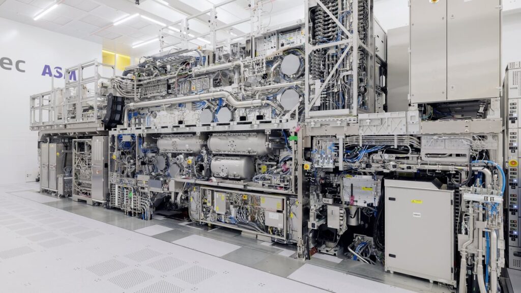
ASML has secured agreements from TSMC, Samsung, and Intel to adopt its newest High-NA EUV lithography machines. The Dutch firm is the sole global manufacturer of this equipment, which is essential for building the most powerful AI accelerators. Samsung intends to deploy the technology for high-volume manufacturing in 2028, with TSMC following in 2030. Intel already operates the systems. A single unit costs up to $400 million.
Four-inch masks aim to boost throughput by 40 percent
The deal relies on a shift in photomask size. The four companies plan to move from the current six-inch standard to twelve inches. A photomask acts as a stencil holding a chip’s circuit pattern. In lithography, light passes through this mask onto a silicon wafer coated with light-sensitive material. This transfers the pattern onto the wafer, where transistors and circuit paths form.
The larger mask allows imaging of more area in a single exposure. The six-inch limit previously capped chip size, forcing manufacturers to stack chips vertically and connect them in complex ways. This drove up cost and complexity.
ASML technology chief Marco Pieters called the switch a huge opportunity. He noted it could raise High-NA machine throughput by 40 percent and simplify the design process. TSMC and ASML plan to build a test line for twelve-inch masks by 2031, with production use on High-NA tools set for 2033.
TSMC was cautious until now, arguing productivity gains did not yet justify higher costs. The company is now reversing course. TSMC accounts for about 16 percent of ASML’s revenue. Together with Samsung and Intel, the three largest customers are on board. Samsung is one of the largest memory makers and plans to use High NA for memory chips starting in 2028. Prices for these chips are climbing sharply right now because of demand from AI data centers.
Huawei orchestrates China’s answer to ASML dependence
Meanwhile, Huawei is pushing to strip foreign technology out of China’s semiconductor supply chain. The company works around Western export controls that cover ASML’s valuable technology, according to a report from the Financial Times. Huawei is investing across the entire lithography chain and helping broker deals with leading fabs like SMIC.
China is not focused on the most advanced EUV technology, but on DUV. The abbreviation stands for Deep Ultraviolet, with a wavelength of 193 nanometers. EUV works at a much shorter 13.5 nanometers. The shorter wavelength allows finer structures and therefore the most advanced chips. DUV is the older, more mature technology and is used for most chips made worldwide. With so-called multi-patterning, where a pattern is built up over several exposure steps, it can also produce more advanced semiconductors. This approach requires greater effort and cost than EUV.
At the center of Huawei’s effort is Yuliangsheng, a Shanghai equipment maker that helped develop China’s first advanced DUV machine, according to the FT. The company was spun out of SiCarrier, which the FT says has close ties to Huawei. Huawei denies this claim. The machine is being tested by SMIC and on Huawei’s own production lines, so far for less complex semiconductors. Yuliangsheng aims to produce twelve DUV machines by the end of the year, but remains far behind ASML.
Bernstein analyst Lin Qingyuan said Huawei plays a project management role in China’s DUV push. He noted that a DUV prototype alone is not enough. You need thousands of suppliers and customers working together, plus a central orchestrating force.
The biggest bottlenecks remain projection lenses and light sources. Yuliangsheng uses lenses from Zeiss, according to the FT. The company said it sells its optics only to ASML. But insiders point to the secondary market. Huawei’s venture capital arm Habo is at the same time backing Zeiss rivals like Fujian Zhiqi Photonics and light-source developer Beijing RSLaser to become more independent here too.
What it means
For engineers building AI hardware, the shift to twelve-inch masks means faster production runs and simpler chip layouts. The current six-inch limit forced complex stacking solutions that increased cost. Removing that constraint allows for larger, more efficient dies. For the teams at TSMC and Samsung, this validates their investment in High-NA tools and aligns their timelines with the growing demand for memory and accelerators.
For chipmakers in China, the path forward involves DUV and multi-patterning rather than immediate EUV adoption. Huawei is coordinating a wider ecosystem to reduce reliance on foreign optics and light sources. Backing rivals of Zeiss and other Western suppliers aims to create a more independent supply chain. However, the gap in capability between domestic DUV efforts and ASML’s EUV technology remains significant.