An ambitious chip startup has emerged from stealth mode with a plan to fix the global memory shortage without building new factories.
Kepler Computing, founded in 2018 in San Jose, California, claims its new architecture for high-bandwidth memory (HBM) can bypass the supply bottlenecks currently constraining the computing market.
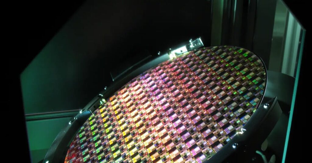
Most chipmakers rely on expensive extreme ultraviolet lithography (EUV) to shrink transistors and pack more technology into smaller spaces. Kepler says its “3D stacking” approach and a proprietary material allow it to increase density without EUV at all, working instead with existing semiconductor fabrication plants.
The company has reported similar gains for high-speed cache memory, or SRAM, used in CPUs, GPUs, and XPUs. This memory sits within the core of a chip die to cut data transfer times. HBM differs by using stacks of DRAM, a separate memory component.
Kepler has raised $468 million from backers including GlobalFoundries, Intel Capital, AMD Ventures, the British fund Baillie Gifford, and Bill Gates through his Gates Frontier fund.
In July, the US Department of Commerce committed up to $245 million to Kepler to develop a new class of high-performance AI memory technology in the US, enabled by innovative 3D and ferroelectric technologies.
Testing is currently happening in Singapore, where GlobalFoundries has a facility. Over the past two years, Kepler has built “mini fabs” to produce its memory chips alongside GlobalFoundries’ 28-nanometer chips. Tests have also run in GlobalFoundries’ facilities in Burlington, Vermont.
Investors say the timing could not be better. The global memory chip shortage highlights two realities: building new fabs is hugely expensive and painstaking, and demand for specific memory types is cyclical. In a data-center-driven, AI-crazed world, HBM has become the standard.
Leading makers like SK Hynix and Micron are racing to build multibillion-dollar fabs to meet demand, wagering that even when operational, the industry will still need high-bandwidth memory.
“For a long time our thinking was that we’d work on SRAM first and then follow up with DRAM and HBM,” says Debo Olaosebikan, Kepler’s cofounder and chief executive officer. “But with the launch of ChatGPT [in 2022] and the explosion of demand for an HBM alternative, we started working on our HBM road map. Now we’re making SRAM and HBM in parallel.”
“We didn’t go in thinking that this would be a replacement for DRAM or a replacement for SRAM,” says Srini Ananth, managing director at Intel Capital. “We figured the market would dictate that, and now you’re seeing a demand for both.”
By bypassing ultraviolet lithography, Kepler joins a few startups working to avoid a major manufacturing bottleneck. The startup claims it can produce SRAM with the same density as 2-nanometer or 3-nanometer chips without investing in EUV.
“Kepler’s approach is at the sweet spot of our strategy,” says Ed Kaste, senior vice president of GlobalFoundries’ CMOS business. “It’s a new materials system, with multigenerational scaling potential, without having to build entirely new systems in the fab or invest in very expensive lithography equipment.”
Material Impact
Kepler argues the accelerated computing market should not wait for brand-new memory fabs to meet demand. Instead, new approaches to building memory within existing fabs can increase supply.
Their approach is twofold. For HBM, Kepler has developed a novel 3D-manufacturing technique that fits more memory chips within a fixed footprint. The core compute sits closer to the memory, so data travel uses less energy. The ultimate goal is to move data in HBM with energy comparable to SRAM while keeping HBM’s large capacity.
Kepler also improved SRAM density using ferroelectrics, which read and write data at lower voltages than typical semiconductor mechanisms. The startup developed a new, low-voltage, composite material to work with this approach.
Sasi Manipatruni, Kepler’s cofounder and chief technology officer, says the team went through 35 iterations of composites before landing on a material class that would make memory chips easier and cheaper to make.
“Once we found a way to solve the physics problem—as in the physical limitations for HBM—we came up with a material innovation that helps with the amount of memory you can have between chips,” he says.
In early builds with GlobalFoundries, Kepler converted a fab into a “next-generation” fab in eight months, compared to a typical 24-month timeframe.
“Our goal is to take the fabs and architectures already built, and push them to the limits of physics,” Olaosebikan says.
Kepler bets that additional costs from new materials or retooling existing fabs would far outweigh the $20 billion to $40 billion it costs to build new ones and outfit them with equipment worth hundreds of millions of dollars.
Waiting to Scale
Kepler Computing still has a long road ahead before reaching full-scale production. To date, the company has run its technology on around 2,000 wafers. The startup plans to ship its first samples of HBM chips later this year, ramp up production out of Singapore next year, and start chip production in the US in 2028.
Kaste says he is confident the “fundamental breakthroughs have happened. What remains is getting good results on thousands of wafers and millions of devices.”
One challenge with this material system is that it includes iron in its composite. “Iron is a tough contaminant to introduce into a production facility. So Kepler’s solution has to run on dedicated equipment, or be fully encapsulated so that it can’t escape,” Kaste says.
“The art is in keeping that material really well isolated through our production flow,” Kaste says.
Olaosebikan would not confirm the specific elements of the composite material. “What I can say is, we’re using a small number of materials, and some of them aren’t what you’d typically find in mainstream ferroelectrics,” he says.
Kepler is not the only startup looking to upend the semiconductor industry. Late last year, a well-funded startup called Substrate made waves for its new approach to lithography, which uses nanoparticles to etch details onto advanced chips. Some industry analysts were skeptical of the startup’s ambitions, noting it would be extremely difficult to produce a large number of chips “that meet incredibly stringent specifications, on time and on budget,” as reported in Bloomberg.
Scale is a common challenge when attempting to innovate semiconductor manufacturing, whether with new processes, materials, or some combination of both. “The question is how to overcome all the limitations of contamination, different materials, and different tooling, in such a way that the resulting innovation can be used at scale and is worth the cost,” says Austin Lyons, a chip analyst for Creative Strategies, who was not briefed on Kepler’s innovation.
Proving out a new method for memory is one thing; meeting the historic demand for it will be another altogether.