
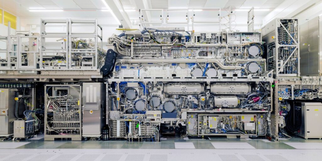
Jos Benschop climbs a ladder to inspect the top of a machine that weighs more than 150 tons and spans the length of a double-decker bus.
The device is covered in snaking tubes, pressurised tanks, and thousands of cables. From the ground, it resembles a futuristic V8 engine. When Benschop reaches the top, he and the author look down from 15 feet above bunny-suited technicians scurrying around the floor.
Benschop, a 66-year-old executive vice president of technology at ASML, describes the 200 cubic metres of equipment as mechatronic devices holding mirrors with atomic precision. He has spent over a decade designing the machine with his engineers but still reacts with disbelief when looking at the finished product.
ASML is a Dutch firm and the essential link in the microchip industry. To build powerful chips for phones or artificial intelligence, manufacturers require a lithography machine. This process involves shining light onto a silicon wafer to pattern the transistors and wiring before they are cut from the wafer.
ASML and TSMC control the chipmaking field. ASML creates the lithography machines, while TSMC, a giant based in Taiwan, uses them to manufacture the vast majority of microchips.
Nine years ago, ASML began selling machines using extreme-ultraviolet light, or EUV. These machines produce radiation by shooting lasers at tiny molten drops of tin tens of thousands of times a second. The original models, the result of a 16-year research project costing about $10 billion, can craft transistor features of 13 nanometres. The new machine improves on this with a resolution of just eight nanometres, roughly the width of 40 silicon atoms. The units are shipping to factories at a price of $400 million each.
Chipmakers pay this amount because they must produce improved chips annually. This requires ever smaller components packed more densely to create faster and more energy-efficient hardware.
ASML’s tools have been critical to maintaining Moore’s Law. Without this advanced technology, chip density and the ability to perform calculations would likely have plateaued.
The artificial intelligence industry has created a ravenous demand for denser chips. Firms like OpenAI and Anthropic are building server farms to train and deploy new models, requiring increasingly powerful hardware. ASML’s latest machine aims to support this demand for at least another decade.
“We can allow customers to go to smaller and smaller features, and that opens up the space for whatever we see now today in AI, which is absolutely mind-blowing,” Marco Pieters, ASML’s chief technology officer, said. “I think we’ve only seen the tip of the iceberg.”
ASML’s relentless push for shrinkage has made it a dominant force. The company produces about 90% of all chip-lithography tools worldwide. If you make chips, ASML is unavoidable.
This monopoly position causes concern for some governments. The duopoly of ASML and TSMC has geopolitical implications. In an effort to prevent China from developing advanced AI, the US government pressured the Dutch government to impose an embargo in 2019. ASML is forbidden from selling high-end machines to any Chinese firm.
James Proud, the cofounder and CEO of the lithography startup Substrate, says the situation is not ideal. The US is dangerously reliant on a supply chain that is overseas and increasingly expensive. There is a huge concentration in a small number of players, and the supply chain is very expensive.
After two decades of ASML’s dominance, competitors are now targeting its territory. China is pouring billions into replicating the technology. Startups like Substrate are trying to create lithography machines that are cheaper, smaller, and more capable. The near future clearly belongs to ASML, but as its engineers know, a giant can be unseated with the right trick.
How the machine works
Chipmaking resembles silk-screening a T-shirt. A pattern on a reticle, or mask, is transferred to a silicon wafer by shining light on it. The light interacts with chemicals on the wafer to fix the pattern in place.
The size of a chip’s features is partly set by the wavelength of light used. A smaller wavelength allows for smaller circuitry. Engineers can stretch capabilities by increasing the numerical aperture, usually by swapping in a bigger lens. Eventually, this trick hits a limit, and a new form of light with a smaller wavelength is required.
History shows a two-step dance. The industry finds a good light source, increases the numerical aperture, and then accepts the need for a smaller wavelength before restarting the cycle. Up to the early 1990s, chipmakers used visible light with a wavelength of about 400 nanometres. By the mid-1990s, they upgraded to deep ultraviolet, reaching a 193-nanometre wavelength. By the late 1990s, the end of the line for deep ultraviolet approached.
Options were troublesome. X-rays offered a one-nanometre wavelength but were devilishly hard to focus. Beams of electrons and ions were precise but worked like dot-matrix printers, transferring patterns point by point, which was far too slow. The industry wants a machine to crank out hundreds of wafers per hour.
Around 2001, ASML, then a smaller player, bet on EUV with a wavelength just shy of the x-ray range. Nikon and Canon worked on it as well but dropped out while ASML kept going. The idea was full of unknowns. Nobody knew how to reliably generate that type of light or how to focus it, as EUV is absorbed by regular glass lenses and even air. ASML estimated it would take six full years to wade through this research nightmare.
In reality, it took 16 years and about $10 billion in research. The machine works in a vacuum, creating EUV light by vaporising molten tin and using mirrors to direct it. Zeiss, a historic German optics company, invented new techniques for polishing and inspecting the mirrors, using an ion beam to knock off minute imperfections.
“They sort of ignored the buzz of, like, ‘Hey, this is never gonna work’, and they just beat their heads against these huge engineering problems,” Jeff Koch, an analyst for SemiAnalysis who used to work for ASML, said. “It’s a very engineering-heavy company: ‘Let’s send thousands of engineers and just have them mow down these problems.’ That’s what they did, and it worked.”
When the first EUV machines went on the market in 2017, they cost well over $100 million apiece. Observers wondered if demand would exist from major chipmaking firms like TSMC, Samsung, and Intel. In the years chipmakers waited for EUV, the industry developed clever ways to improve old-fashioned deep ultraviolet light. Maybe EUV would not be needed for a while?
ASML lucked out. Only a few years after EUV debuted, OpenAI released GPT-3 and then ChatGPT. Artificial intelligence burst into the mainstream. Firms like OpenAI, Google, Meta, and Anthropic became hungry for increasingly high-end chips as they built massive server farms. EUV made it easier and faster to crank out AI-tailored chip designs. Nvidia began producing elite GPUs suited for AI training that cost $40,000 each, and big companies could not get enough.
The AI wars were on, and EUV was in demand. In 2025, ASML says it sold nearly 50 EUV machines to companies and pulled in nearly $40 billion in revenue. As of press time, the company’s market cap was over half a trillion dollars.
What it means
ASML’s new machines have potential customers, but one in particular cannot buy them for any amount of money: China.
The US wants to hobble China’s ability to create cutting-edge AI chips or any advanced chips. When ASML began selling its original EUV machines in 2017, the Trump administration successfully pressured the Dutch government to forbid sales to Chinese firms. The US had also imposed export controls on China’s telecom giant Huawei, banning US firms from using its 4G and 5G equipment.
This one-two punch incensed the Chinese government and stirred it to action. China is now pouring billions into catching up and developing its own EUV chip-patterning technology. A Reuters report last winter found that a government skunkworks employing former ASML staffers had cobbled together a machine so huge it filled the entire floor of a lab. It is unclear how well it works. The experiment may be making some chips, but it is doubtful it can do so at an industrial scale.